This project, the code, and diagrams can be found at https://github.com/aryanka15/FPGA_Image_Processor (this article describes the project up to commit 228c03)
Introduction
Over the past couple of months I've been trying to get better at FPGA design, ever since I got completely lost while interviewing for an FPGA design internship position. FPGAs are Field Programmable Gate Arrays, a large grid of programmable logic blocks and interconnected wires that can represent ANY digital logic circuit. I'm not going to go into how they work in too much detail, but the main advantage to FPGAs is their flexibility.
I had to do something simple enough that I could finish it in a couple of months without using too many tutorials, but also interesting enough to see myself make significant progress. As a photographer, image and video processing will always be interesting to me, so I decided to go down that route. My aim is to create a Image Convolution Accelerator.
Theory
Images can be manipulated using 'kernels', a fancy word for a matrix of weights that are applied to an image's pixels. For simplicity, consider a 3x3 matrix. This 3x3 matrix, along with a 3x3 pixel 'cutout' of an image, can be used to perform a convolution. This is done by doing an element-wise multiplication of the kernel and 3x3 image matrix, then summing the results.
The sum is the value of the pixel in a new image. Imagine this 3x3 kernel sliding across an image, performing convolution at each shift, and using the new value as a pixel, creating an entirely new image. This is what I wanted my hardware to do.
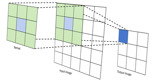
Source: https://medium.com/@timothy_terati/image-convolution-filtering-a54dce7c786b
Depending on the kernel used, different filters can be applied like edge detection, emboss filters, blur filters, and more. The only downside is that your image resolution will decrease, as seen above. The pixels on the edges never get processed, as they can never be the center of a 3x3 cutout of the image, so they are simply cropped.
Project Goals
I was recently introduced to RTL through my ASIC Design Lab and Intro to Digital Design classes, so my goals needed to be realistic. This project didn't need to be super robust, or compatible with microprocessors, AHB/APB/AXI control, or anything super special. Iteration 1 needed to have this basic functionality: run a convolution filter using a 3x3 kernel on a 512x512 grayscale image. These are the main components I needed to design:
- Controller - Something to handle data loading, activating the "math" module, and keeping the device IDLE when nothing is happening
- Data Buffer - A FIFO to load 512 pixels of data, which are 1 byte each.
- MAC - Multiply and Accumulate module, to handle the matrix multiplication and overflow handling, providing the output pixel for each convolution
- Shift Registers - Something to hold the current "window" of the image. A shift register is perfect, because a sliding window is just shifting through the image. The controller would need to make sure the shifting happens at the right times.
I'm writing this after I've done a lot more on the project, but this is how I started-I'm trying to document the whole design process from start to finish as accurate as I can.
Tools
I don't have a real FPGA with me, but luckily AMD/Xilinx provides a free tool, Vivado, to write and simulate RTL on a virtual FPGA. It will even show you the physical resources that your design uses, down to the register. You can run behavioral simulation (which essentially runs your code) and post-implementation simulation (which tests your design while simulating logic gate delays, register delays, setup/hold times, etc.)
I'm going to use draw.io to create RTL diagrams, because everything is a little easier with a bit of visualization. Also, it's great to have diagrams for documentation.
Obviously, I'm going to be using GitHub and Git for version control.
Designing and Diagramming
Note: I went through a few iterations while debugging my design. Also, there were significant performance improvements over time, but I'm going to start with the most basic design that I created.
Top Level
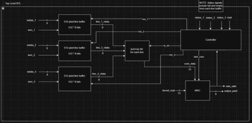
The accelerator will consist of 3 line buffers with 512 pixels of storage each. Each have their own data input and enable signals. The write enable comes from the user/SoC and the read enable is driven by the controller. The read data from each buffer is fed into a shift register, whose enable is also driven by the controller. The shift register holds our "window" that the convolution will take place in.
The MAC performs the convolution math. In this design, assume the kernel matrix is hardcoded into the design (it actually still is in the latest version, I intend to change that soon).
The controller is an FSM (Finite State Machine) that handles the changing output signals based on the flow of data and processing to control the line buffers, shift registers, and MAC.
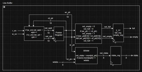
Line Buffer
There's a lot of pseudocode in this design, I'm trying to reduce that in my diagrams.
This line buffer uses an inferred BRAM (Block RAM) to store 512 bytes on the FPGA. The rest of the logic is read/write logic and pointer logic. Essentially, the line buffer keeps track of a read pointer and a write pointer, which go from 0 to 511. There is an extra bit to help with empty/full logic, because these pointers can wrap around, and we need to make sure that we don't write to a full buffer or read from an empty buffer.
The buffer performs a read/write when the corresponding enable signal is high on the clock. I should have added some error state if both enable signals were high, but since this is a personal project, I decided to skip that at the moment.
MAC (Math module)
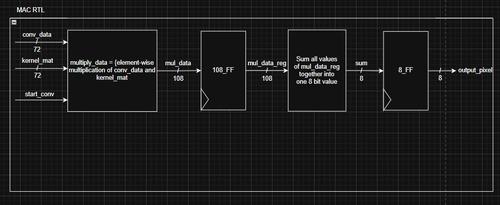
This is the MAC. It is a pipelined design, which uses 9 parallel multipliers for the element-wise matrix multiplication. Then, a large adder sums the values together. The adder is a HUGE combinational block, and needed to be split into one more pipelined stage later on. This is because I was doing 16-bit addition, which and each adder past the first bit needs the carry over from the previous bit, adding to gate delay, and reducing clock speed.
A mistake I made was not taking advantage of this pipelining in the controller in my first iteration, but it was a good experiment to see how much pipelining can really boost performance.
Controller
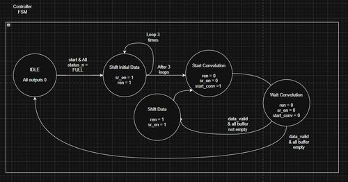
This controller is just a common state machine. It sits at IDLE until a start signal from the SoC, AND the buffers need to be full. Then, it shifts the initial 3x3 window, performs a convolution, shifts by one, and repeats until the buffers are empty. A few things to note is that this controller and the overall design assume a 512 pixel image and 3x3 kernel. Making these flexible (in theory) seems like a daunting task that I may or may not take on. I don't want to be stuck on one personal project for too long.
You can see that, for each convolution, there is a Wait Convolution state, which is completely against the idea of pipelining. Pipelining allows you to input data before the previous data has finished processing, because there are registers which hold the intermediate data in each clock cycle.
Results
This design was decent, and also disappointing. It finished a convolution of an image in 20 ms. It's fast, but a C program can do it way faster. That kind of makes sense, considering a CPU runs at GHz clock speeds, and this runs at 200 MHz.
I was able to get my FPGA, in its final iteration, to run the convolution in 1ms, 1 pixel per clock cycle... which is the same time as a C program. That's pretty good considering the massive gap in clock speeds, but the FPGA can do even better. It's all about architecture.