This project, the code, and diagrams can be found at https://github.com/aryanka15/FPGA_Image_Processor (this article describes the project up to commit a05305 ).
If you haven't already, go ahead and read Parts 1 and 2 on my blog, then come back here. If you have, here's a quick recap.
Recap
I optimized the accelerator to run a convolution in about 1.3 ms, which translates to processing images at just over 700 FPS. This was done by taking advantage of the pipelined MAC using the controller, and implementing the rolling buffer to load our next line of pixels while the convolution is taking place. The accelerator is fast, but software can match this speed in a optimized C program.
To further optimize the accelerator, I needed to take advantage of the parallelization that custom hardware provides.
Parallelization
At the moment, our architecture uses one MAC unit to output one pixel per clock cycle. This is fine, but what if we just used more MACs, performing multiple convolutions in parallel, to output more than 1 pixel per clock cycle. The question is, how many?
One pixel in a black and white bitmap image is 8 bits. Modern microprocessor architecture generally uses 32-bit data, like the RP2040. So, if we used four MACs, we would be processing 32 bits per cycle, which is the most efficient use of our microprocessor's throughput capacity. This also means the accelerator will read in four pixels per cycle to avoid stalling for data to be read.
Architecture Changes
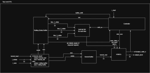
The line buffers, shift registers, and MAC need to be changed to handle 32 bit buses rather than 8 bit buses. Additionally, the MAC needs to run 127 convolutions rather than 510 convolutions, so the buffer shift counter in the controller is adjusted as well.
Once four MACs are instantiated, the convolution data will need to be routed to each MAC. The convolutions for four consecutive pixels will be executed in parallel.
The new 32-bit buses plus extra stage of pipelining (I'll explain why soon) caused further delays for the last few convolutions, and extra FSM states were added to handle the trailing data outputs.
Here is the new architecture:
The Kernel Buffer was used to implement dynamic kernel loading. This wasn't too difficult, it is just a shift register that takes a 24-bit input (one row of a 3x3 kernel) per cycle.

These are the main changes, other components simply had a 8 bit -> 32 bit bus conversion, while logic stayed the same.
Challenges
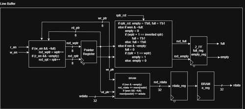
The most critical challenge that came with this design is the net and logic delays that it introduced. Net delay is the time it takes for a signal to travel the length of a wire, and in this case, there were too many long wires. The convolution data was traveling from BRAM, to an output register, and then back towards the multiplication logic which was placed farther from the register than the BRAM.
The second issue was that a change in the kernel data shift register propagated directly through the multiplication logic, which took too long.
Fix #1 - BRAM Output Register
A Xilinx FPGA's BRAM has a built-in output register to avoid using a new on-chip flip flop. Unfortunately, this added a one-cycle delay for rdata to appear on the output, so a few cycles were added to the overall convolution process. If you look at the code, the ren && ~empty logic controls data from the BRAM to a "next data" register. However, regardless of ren and empty, the rdata is updated from the "next data" register. This is why the controller has a Wait Read and extra ren signal in Last Data.
Fix #2 - Using DSPs
The multiplication logic was 6 logic levels deep, which caused a logic delay of just over 2ns. Combined with the net delay of the BRAM to the multiplication logic, I was failing timing by about 0.5ns. To fix this, I forced Vivado to place the multiplication logic in DSPs, removing all asynchronous resets to conform to DSP inference requirements. DSPs (Digital Signal Processing units) are very fast multipliers and adders built into an FPGA, which dropped the logic level from 6 to 0.
But I was still failing timing by -0.02 ns. When I looked at the implementation, this was because the convolution data was in a BRAM, but the kernel data was using a shift register, and any change in kernel data immediately propagated through the DSP, which took just a little too long.
Fix #3 - Extra Pipeline
I added registers to hold the convolution and kernel data to the MAC, placing the inputs close to the DSP and adder logic, reducing net delays and finally meeting timing requirements. This was when I was finally able to run a post-implementation timing simulation without glitches and metastability. Of course, this added an extra cycle because each convolution data would take an extra cycle to hit the MAC logic, but this was negligible due to the pipelined nature of the device.
Final
The final product is a 512x512 image convolution accelerator that has a configurable 3x3 kernel. The accelerator performs one convolution in about 0.0035 seconds, or 0.35 ms.
The applications for this are extensive, from CNN acceleration to noise reduction and other image/video filtering inside cameras like my own Nikon D5600.
This project taught me a lot about how to make efficient, low power accelerators for simple tasks, and I hope to continue iterating on this project, integrating it with an AXI bus, expanding to RGB image convolution, running object detection filters, and also refactoring the accelerator to support video streams, either from a microprocessor or camera HDMI streams.
However, I don't want to stay on one project too long, and will likely shelve this proejct for now, as there's a lot more to explore in the world of Computer Engineering, from embedded systems to computer architecture.
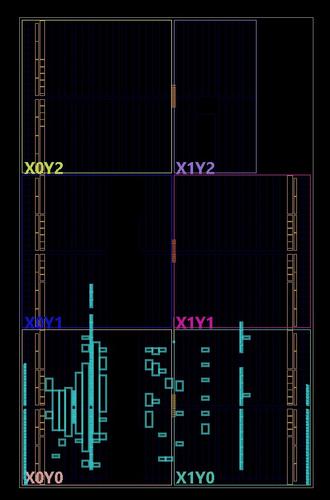
FPGA usage after implementation.